- ALL COMPUTER, ELECTRONICS AND MECHANICAL COURSES AVAILABLE…. PROJECT GUIDANCE SINCE 2004. FOR FURTHER DETAILS CALL 9443117328
Projects > ELECTRONICS > 2017 > IEEE > VLSI
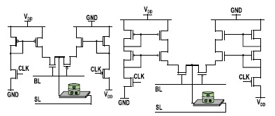
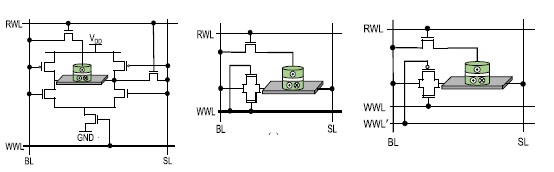
In this paper, various energy-efficient write schemes are proposed for switching operation of spin hall effect (SHE)-based magnetic tunnel junctions (MTJs). A transmission gate (TG)-based write scheme is proposed, which provides a symmetric and energy-efficient switching behavior. We have modeled an SHE-MTJ using precise physics equations, and then leveraged the model in SPICE circuit simulator to verify the functionality of our designs. Simulation results show the TG-based write scheme advantages in terms of device count and switching energy. In particular, it can operate at 12% higher clock frequency while realizing at least 13% reduction in energy consumption compared to the most energy-efficient write circuits. We have analyzed the performance of the implemented write circuits in presence of process variation (PV) in the transistors’ threshold voltage and SHE-MTJ dimensions. Finally, we have proposed the 1TG-1T-1R SHE-based magnetic random access memory (MRAM) bit cell based on the TG-based write circuit.
Negative Bitline Technique.
In this paper, we developed a symmetric energy-efficient TG-based write scheme for SHE-based MTJ devices. An SHE-MTJ Verilog-A behavioral model was leveraged via SPICE circuit simulations to validate the functionality of the designed circuit using experimental parameters. Various write schemes were developed and equipped with clocking mechanism to produce the required bidirectional current for SHE-MTJ switching. Simulation results exhibit symmetric behavior of the proposed TG-based write circuit. Comparisons with various write schemes indicated that TG-based design excels in terms of switching delay and energy. We have investigated the functionality and performance of implemented write circuits in presence of PV in the transistors’ threshold voltage and SHE-MTJ dimensions. The obtained results showed that the proposed TG-based design is the second most PV-resilient SHE-MTJ write circuit among the implemented designs, allowing appropriate energy versus PV tradeoffs. Finally, we have leveraged three of the most energy-efficient and PV-resilient write circuits within a memory bit cell, and investigated their energy and area tradeoffs. Obtained results exhibit that our proposed 1TG-1T-1R SHE-MRAM bit cell excels in term of EDP, while incurring low area overhead.
Developed current mirror write circuits
Developed current mirror read circuits